1. Essential Features and Nanoscale Habits of Silicon at the Submicron Frontier
1.1 Quantum Confinement and Electronic Framework Improvement
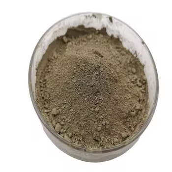
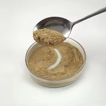
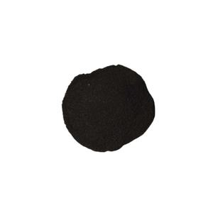
(Nano-Silicon Powder)

Nano-silicon powder, made up of silicon fragments with characteristic dimensions below 100 nanometers, stands for a standard shift from mass silicon in both physical actions and functional utility.
While bulk silicon is an indirect bandgap semiconductor with a bandgap of around 1.12 eV, nano-sizing causes quantum confinement results that essentially change its electronic and optical buildings.
When the bit diameter methods or drops listed below the exciton Bohr radius of silicon (~ 5 nm), cost carriers become spatially confined, resulting in a widening of the bandgap and the development of noticeable photoluminescence– a sensation missing in macroscopic silicon.
This size-dependent tunability makes it possible for nano-silicon to release light across the visible spectrum, making it an appealing candidate for silicon-based optoelectronics, where standard silicon falls short due to its bad radiative recombination performance.
In addition, the raised surface-to-volume ratio at the nanoscale boosts surface-related sensations, consisting of chemical reactivity, catalytic activity, and interaction with magnetic fields.
These quantum effects are not merely scholastic interests but create the structure for next-generation applications in power, picking up, and biomedicine.
1.2 Morphological Variety and Surface Chemistry
Nano-silicon powder can be manufactured in numerous morphologies, including round nanoparticles, nanowires, porous nanostructures, and crystalline quantum dots, each offering unique advantages depending upon the target application.
Crystalline nano-silicon generally maintains the ruby cubic framework of mass silicon but shows a greater thickness of surface area flaws and dangling bonds, which need to be passivated to support the product.
Surface functionalization– frequently accomplished through oxidation, hydrosilylation, or ligand add-on– plays a critical function in determining colloidal security, dispersibility, and compatibility with matrices in compounds or biological settings.
For instance, hydrogen-terminated nano-silicon shows high sensitivity and is prone to oxidation in air, whereas alkyl- or polyethylene glycol (PEG)-covered fragments show enhanced stability and biocompatibility for biomedical usage.
( Nano-Silicon Powder)
The visibility of a native oxide layer (SiOₓ) on the particle surface, even in very little quantities, substantially affects electrical conductivity, lithium-ion diffusion kinetics, and interfacial reactions, particularly in battery applications.
Recognizing and regulating surface area chemistry is as a result crucial for taking advantage of the full possibility of nano-silicon in useful systems.
2. Synthesis Strategies and Scalable Fabrication Techniques
2.1 Top-Down Approaches: Milling, Etching, and Laser Ablation
The production of nano-silicon powder can be broadly categorized into top-down and bottom-up approaches, each with unique scalability, pureness, and morphological control characteristics.
Top-down methods involve the physical or chemical decrease of mass silicon right into nanoscale fragments.
High-energy sphere milling is a commonly utilized industrial approach, where silicon chunks undergo intense mechanical grinding in inert ambiences, leading to micron- to nano-sized powders.
While cost-efficient and scalable, this method usually presents crystal problems, contamination from crushing media, and wide fragment size distributions, calling for post-processing purification.
Magnesiothermic reduction of silica (SiO TWO) followed by acid leaching is another scalable path, especially when using natural or waste-derived silica sources such as rice husks or diatoms, supplying a lasting path to nano-silicon.
Laser ablation and reactive plasma etching are much more exact top-down techniques, capable of producing high-purity nano-silicon with controlled crystallinity, however at higher price and lower throughput.
2.2 Bottom-Up Techniques: Gas-Phase and Solution-Phase Development
Bottom-up synthesis allows for higher control over fragment size, shape, and crystallinity by constructing nanostructures atom by atom.
Chemical vapor deposition (CVD) and plasma-enhanced CVD (PECVD) allow the development of nano-silicon from aeriform forerunners such as silane (SiH ₄) or disilane (Si two H SIX), with criteria like temperature, pressure, and gas flow determining nucleation and growth kinetics.
These approaches are particularly effective for creating silicon nanocrystals embedded in dielectric matrices for optoelectronic devices.
Solution-phase synthesis, including colloidal courses using organosilicon compounds, permits the manufacturing of monodisperse silicon quantum dots with tunable emission wavelengths.
Thermal decomposition of silane in high-boiling solvents or supercritical liquid synthesis additionally generates top notch nano-silicon with slim size distributions, suitable for biomedical labeling and imaging.
While bottom-up methods normally create remarkable material quality, they encounter obstacles in large-scale manufacturing and cost-efficiency, requiring continuous research into crossbreed and continuous-flow processes.
3. Power Applications: Revolutionizing Lithium-Ion and Beyond-Lithium Batteries
3.1 Role in High-Capacity Anodes for Lithium-Ion Batteries
One of one of the most transformative applications of nano-silicon powder depends on energy storage space, particularly as an anode material in lithium-ion batteries (LIBs).
Silicon uses a theoretical certain capability of ~ 3579 mAh/g based upon the formation of Li ₁₅ Si Four, which is virtually 10 times higher than that of conventional graphite (372 mAh/g).
However, the large quantity growth (~ 300%) throughout lithiation causes fragment pulverization, loss of electrical call, and continuous strong electrolyte interphase (SEI) development, resulting in fast capability discolor.
Nanostructuring minimizes these problems by shortening lithium diffusion courses, fitting strain better, and minimizing crack probability.
Nano-silicon in the kind of nanoparticles, permeable frameworks, or yolk-shell frameworks makes it possible for relatively easy to fix biking with boosted Coulombic efficiency and cycle life.
Business battery modern technologies now integrate nano-silicon blends (e.g., silicon-carbon compounds) in anodes to improve energy thickness in customer electronic devices, electric vehicles, and grid storage systems.
3.2 Possible in Sodium-Ion, Potassium-Ion, and Solid-State Batteries
Beyond lithium-ion systems, nano-silicon is being explored in emerging battery chemistries.
While silicon is much less reactive with sodium than lithium, nano-sizing boosts kinetics and enables restricted Na ⁺ insertion, making it a candidate for sodium-ion battery anodes, specifically when alloyed or composited with tin or antimony.
In solid-state batteries, where mechanical stability at electrode-electrolyte interfaces is critical, nano-silicon’s capacity to go through plastic deformation at small ranges lowers interfacial stress and enhances contact maintenance.
Additionally, its compatibility with sulfide- and oxide-based strong electrolytes opens up avenues for much safer, higher-energy-density storage options.
Research study remains to optimize interface engineering and prelithiation methods to take full advantage of the longevity and effectiveness of nano-silicon-based electrodes.
4. Emerging Frontiers in Photonics, Biomedicine, and Composite Materials
4.1 Applications in Optoelectronics and Quantum Source Of Light
The photoluminescent residential properties of nano-silicon have actually renewed initiatives to establish silicon-based light-emitting devices, an enduring difficulty in integrated photonics.
Unlike mass silicon, nano-silicon quantum dots can display reliable, tunable photoluminescence in the noticeable to near-infrared array, making it possible for on-chip lights compatible with corresponding metal-oxide-semiconductor (CMOS) technology.
These nanomaterials are being incorporated right into light-emitting diodes (LEDs), photodetectors, and waveguide-coupled emitters for optical interconnects and noticing applications.
In addition, surface-engineered nano-silicon exhibits single-photon discharge under certain issue configurations, placing it as a potential platform for quantum data processing and secure interaction.
4.2 Biomedical and Environmental Applications
In biomedicine, nano-silicon powder is gaining interest as a biocompatible, biodegradable, and non-toxic alternative to heavy-metal-based quantum dots for bioimaging and drug shipment.
Surface-functionalized nano-silicon bits can be made to target certain cells, launch healing representatives in response to pH or enzymes, and supply real-time fluorescence tracking.
Their deterioration right into silicic acid (Si(OH)₄), a naturally occurring and excretable compound, reduces long-lasting poisoning issues.
Additionally, nano-silicon is being explored for ecological removal, such as photocatalytic destruction of pollutants under noticeable light or as a lowering agent in water therapy processes.
In composite products, nano-silicon boosts mechanical stamina, thermal security, and use resistance when incorporated into metals, ceramics, or polymers, especially in aerospace and automobile parts.
In conclusion, nano-silicon powder stands at the intersection of fundamental nanoscience and industrial technology.
Its special mix of quantum effects, high reactivity, and adaptability throughout energy, electronic devices, and life sciences underscores its role as a crucial enabler of next-generation technologies.
As synthesis strategies development and combination challenges are overcome, nano-silicon will remain to drive development towards higher-performance, sustainable, and multifunctional material systems.
5. Provider
TRUNNANO is a supplier of Spherical Tungsten Powder with over 12 years of experience in nano-building energy conservation and nanotechnology development. It accepts payment via Credit Card, T/T, West Union and Paypal. Trunnano will ship the goods to customers overseas through FedEx, DHL, by air, or by sea. If you want to know more about Spherical Tungsten Powder, please feel free to contact us and send an inquiry(sales5@nanotrun.com).
Tags: Nano-Silicon Powder, Silicon Powder, Silicon
All articles and pictures are from the Internet. If there are any copyright issues, please contact us in time to delete.
Inquiry us


