1. Crystal Structure and Layered Anisotropy
1.1 The 2H and 1T Polymorphs: Architectural and Digital Duality
(Molybdenum Disulfide)

Molybdenum disulfide (MoS ₂) is a layered transition steel dichalcogenide (TMD) with a chemical formula consisting of one molybdenum atom sandwiched between 2 sulfur atoms in a trigonal prismatic sychronisation, creating covalently bonded S– Mo– S sheets.
These private monolayers are piled up and down and held together by weak van der Waals pressures, making it possible for simple interlayer shear and exfoliation down to atomically thin two-dimensional (2D) crystals– a structural attribute central to its varied functional roles.
MoS ₂ exists in numerous polymorphic types, one of the most thermodynamically stable being the semiconducting 2H phase (hexagonal symmetry), where each layer exhibits a straight bandgap of ~ 1.8 eV in monolayer kind that transitions to an indirect bandgap (~ 1.3 eV) wholesale, a phenomenon critical for optoelectronic applications.
On the other hand, the metastable 1T phase (tetragonal proportion) embraces an octahedral control and behaves as a metallic conductor as a result of electron donation from the sulfur atoms, enabling applications in electrocatalysis and conductive composites.
Phase changes between 2H and 1T can be caused chemically, electrochemically, or via pressure design, providing a tunable platform for designing multifunctional tools.
The capability to maintain and pattern these stages spatially within a single flake opens paths for in-plane heterostructures with unique electronic domain names.
1.2 Flaws, Doping, and Side States
The efficiency of MoS ₂ in catalytic and digital applications is very sensitive to atomic-scale problems and dopants.
Inherent point issues such as sulfur jobs act as electron contributors, boosting n-type conductivity and functioning as energetic sites for hydrogen advancement responses (HER) in water splitting.
Grain limits and line flaws can either impede cost transport or create localized conductive paths, depending upon their atomic arrangement.
Regulated doping with change metals (e.g., Re, Nb) or chalcogens (e.g., Se) permits fine-tuning of the band structure, carrier focus, and spin-orbit combining results.
Notably, the sides of MoS ₂ nanosheets, particularly the metal Mo-terminated (10– 10) edges, exhibit significantly higher catalytic activity than the inert basal airplane, inspiring the style of nanostructured drivers with taken full advantage of side exposure.
( Molybdenum Disulfide)
These defect-engineered systems exhibit how atomic-level control can change a normally occurring mineral right into a high-performance practical material.
2. Synthesis and Nanofabrication Methods
2.1 Bulk and Thin-Film Production Techniques
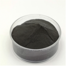
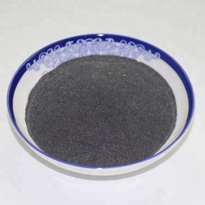
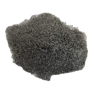
All-natural molybdenite, the mineral kind of MoS TWO, has been used for years as a solid lubricating substance, yet modern-day applications demand high-purity, structurally controlled artificial types.
Chemical vapor deposition (CVD) is the dominant technique for generating large-area, high-crystallinity monolayer and few-layer MoS two films on substratums such as SiO TWO/ Si, sapphire, or versatile polymers.
In CVD, molybdenum and sulfur forerunners (e.g., MoO ₃ and S powder) are vaporized at heats (700– 1000 ° C )under controlled environments, enabling layer-by-layer development with tunable domain size and positioning.
Mechanical exfoliation (“scotch tape approach”) stays a criteria for research-grade samples, yielding ultra-clean monolayers with minimal flaws, though it does not have scalability.
Liquid-phase peeling, including sonication or shear mixing of mass crystals in solvents or surfactant services, produces colloidal diffusions of few-layer nanosheets appropriate for coverings, composites, and ink formulas.
2.2 Heterostructure Assimilation and Tool Patterning
Real potential of MoS two arises when integrated right into upright or lateral heterostructures with various other 2D products such as graphene, hexagonal boron nitride (h-BN), or WSe ₂.
These van der Waals heterostructures allow the design of atomically specific devices, including tunneling transistors, photodetectors, and light-emitting diodes (LEDs), where interlayer fee and power transfer can be crafted.
Lithographic patterning and etching strategies permit the manufacture of nanoribbons, quantum dots, and field-effect transistors (FETs) with network sizes down to tens of nanometers.
Dielectric encapsulation with h-BN secures MoS ₂ from environmental deterioration and reduces cost spreading, significantly enhancing carrier wheelchair and tool security.
These manufacture developments are necessary for transitioning MoS two from laboratory curiosity to feasible part in next-generation nanoelectronics.
3. Practical Qualities and Physical Mechanisms
3.1 Tribological Actions and Strong Lubrication
One of the earliest and most enduring applications of MoS two is as a dry solid lubricating substance in extreme environments where fluid oils stop working– such as vacuum cleaner, heats, or cryogenic problems.
The reduced interlayer shear stamina of the van der Waals gap permits very easy gliding in between S– Mo– S layers, causing a coefficient of rubbing as low as 0.03– 0.06 under optimum problems.
Its performance is further improved by strong bond to steel surfaces and resistance to oxidation approximately ~ 350 ° C in air, beyond which MoO three formation increases wear.
MoS two is extensively used in aerospace mechanisms, vacuum pumps, and weapon elements, commonly used as a coating using burnishing, sputtering, or composite consolidation right into polymer matrices.
Recent studies reveal that humidity can deteriorate lubricity by increasing interlayer bond, triggering study into hydrophobic layers or crossbreed lubricants for improved ecological security.
3.2 Digital and Optoelectronic Reaction
As a direct-gap semiconductor in monolayer form, MoS ₂ displays strong light-matter interaction, with absorption coefficients surpassing 10 ⁵ cm ⁻¹ and high quantum return in photoluminescence.
This makes it ideal for ultrathin photodetectors with rapid response times and broadband level of sensitivity, from noticeable to near-infrared wavelengths.
Field-effect transistors based on monolayer MoS ₂ show on/off ratios > 10 eight and provider movements approximately 500 cm ²/ V · s in suspended examples, though substrate communications typically limit useful worths to 1– 20 cm TWO/ V · s.
Spin-valley coupling, an effect of strong spin-orbit communication and busted inversion proportion, enables valleytronics– a novel standard for information encoding utilizing the valley level of flexibility in momentum space.
These quantum sensations position MoS two as a candidate for low-power logic, memory, and quantum computer elements.
4. Applications in Energy, Catalysis, and Emerging Technologies
4.1 Electrocatalysis for Hydrogen Advancement Reaction (HER)
MoS two has emerged as an appealing non-precious alternative to platinum in the hydrogen advancement reaction (HER), a crucial process in water electrolysis for green hydrogen manufacturing.
While the basal plane is catalytically inert, side websites and sulfur openings show near-optimal hydrogen adsorption cost-free power (ΔG_H * ≈ 0), comparable to Pt.
Nanostructuring techniques– such as creating up and down straightened nanosheets, defect-rich films, or drugged hybrids with Ni or Carbon monoxide– make the most of active website thickness and electrical conductivity.
When integrated into electrodes with conductive supports like carbon nanotubes or graphene, MoS two attains high current densities and lasting security under acidic or neutral conditions.
Additional enhancement is attained by supporting the metal 1T stage, which enhances intrinsic conductivity and subjects extra energetic sites.
4.2 Versatile Electronic Devices, Sensors, and Quantum Gadgets
The mechanical flexibility, openness, and high surface-to-volume ratio of MoS two make it optimal for adaptable and wearable electronics.
Transistors, logic circuits, and memory tools have been demonstrated on plastic substratums, allowing bendable screens, wellness screens, and IoT sensors.
MoS TWO-based gas sensing units exhibit high level of sensitivity to NO TWO, NH SIX, and H ₂ O because of charge transfer upon molecular adsorption, with reaction times in the sub-second range.
In quantum innovations, MoS two hosts localized excitons and trions at cryogenic temperature levels, and strain-induced pseudomagnetic fields can catch service providers, making it possible for single-photon emitters and quantum dots.
These advancements highlight MoS two not just as a useful product yet as a platform for checking out basic physics in minimized dimensions.
In summary, molybdenum disulfide exhibits the convergence of classic products science and quantum engineering.
From its old function as a lubricant to its contemporary deployment in atomically thin electronic devices and energy systems, MoS two remains to redefine the limits of what is feasible in nanoscale products design.
As synthesis, characterization, and combination techniques breakthrough, its effect throughout science and technology is positioned to increase also further.
5. Distributor
TRUNNANO is a globally recognized Molybdenum Disulfide manufacturer and supplier of compounds with more than 12 years of expertise in the highest quality nanomaterials and other chemicals. The company develops a variety of powder materials and chemicals. Provide OEM service. If you need high quality Molybdenum Disulfide, please feel free to contact us. You can click on the product to contact us.
Tags: Molybdenum Disulfide, nano molybdenum disulfide, MoS2
All articles and pictures are from the Internet. If there are any copyright issues, please contact us in time to delete.
Inquiry us


